True Power Research is a power electronics consultant and provider of custom power supply designs. Part of our service and expertise is the design of PCB’s for electronic power supplies.
PCB design is a critical stage in the development of power supplies. The large switching currents are orders of magnitude greater than the sensitive control signal currents used to control the supply. Commingling these very large currents with the small control currents will almost always result in misbehavior. Additionally it is a key consideration to mitigation of both output and input noise. PCB layout of power electronics requires special understanding of how supplies operate along with understanding of all the usual parasitic elements usually operative at switching frequencies.
PCB Design Process for Power Supplies
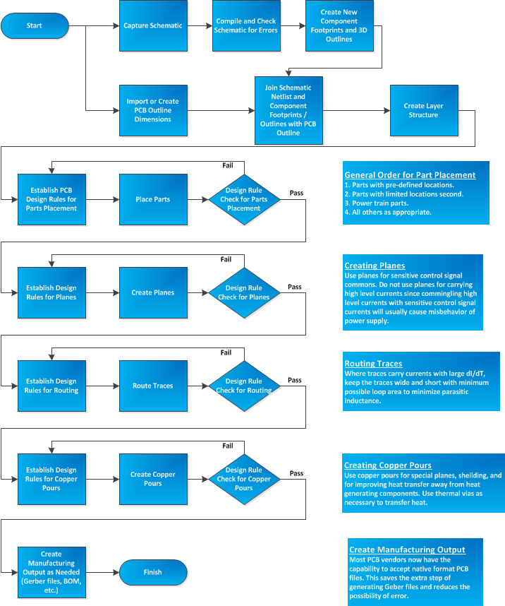
The general work flow for power PCB layout is shown in the following flow chart:
Definitions of PCB Layout Process
Netlist — Information detailing how the electronic parts are interconnected to accheive their functional purpose. The netlist becomes one of the inputs to the PCB document.
Schematic Capture — the process of representing the electronic design in schematic diagram form, from which a netlist of connectivity can be created.
Component Footprint — a 2D representation of the space a component will occupy on the PCB.
PCB Outline — The geographical boundary a PCB assumes and is the limit within which electronic components must be placed.
Layer Structure — Also known as the layer stackup, the arrangement of fiberglass and copper conducting layers which make up the board. There may be numerous internal conducting layers.
Part Placement — The process of locating parts on the PCB. This step in an important step and if done well and thoughtfully will greatly facilitate the successful completion of the board. Therefore, this step should take a significant portion of the PCB layout effort.
Planes — Layers of solid copper dedicated to a common net such as signal common. PCB layout software usually represent planes using inverse video.
Routing — The process of placing interconnecting traces between parts.
Copper Pours — Smaller regions or polygons of solid copper used for various purposes such as shielding, heat transfer, etc. In power electronics, copper pours are often inhabited by thermal vias for heat transfer to other layers.
PCB Design Rule Check — An automated process of examining a PCB design for errors against pre-defined design rules.
Multi-Layer Boards for Power Supply PCB Design / Layout
The advent of switching power supplies brings Power PCB designs with frequency content well into the tens of megahertz. At these frequencies, the parasitic effects of components and PCB traces become prevalent and must be taken into account in the design process. Use of multi-layer PCBs is a must for high performance power supplies to help accommodate these issues. The only time two layer PCBs should be used is when the design is not high performance and the design must be low cost as in consumer products. Otherwise the cost benefit of using a two layer board is negated by performance which will usually not meet the performance specifications.
Power Supply PCB Design Using Altium Designer
True Power Research provides power electronics product design using the market share leading Altium Designer software which includes PCB layout tools. Altium Designer provides in a unified environment all of the basic tools needed to completely design a power supply and streamlines the process to promote work collaboration, component management, and release to manufacturing.
We have the skills and experience for printed circuit board layout for power electronics. Call or email us today for your requirements for power supply PCB design.
Additional References about PCB Design and Layout
For additional information about PCB design from the manufacturers point of view, an excellent resource is the engineering webpage at Advanced Circuits.
For a good text on fabrication of printed circuit boards, see the text Printed Circuit Boards: Design, Fabrication, and Assembly by R.S Khandpur.
Share the Knowledge!
If you benefited from the information on this web page, please share it with others. You have our heartfelt thanks!


